Research
The future of energy supply depends on innovative breakthroughs regarding the design of efficient systems for the conversion of the most available source of renewable energy, solar energy.
Single-junction silicon solar cells are now approaching the practical limit for single-junction solar cells, around 30 %. Their combination with a larger bandgap solar cell in a so-called tandem junction is a promising way to enhance efficiencies.
From 2009, a new class of material for solar cells was discovered: metallorganohalide perovskite. Perovskite solar cells have reached in a few years efficiencies comparable to that of silicon-based cells using abundant and low cost-processed compounds! Their combination with the lower bandgap silicon semiconductor makes it a perfect match for tandem solar cells with complementary light absorption. Calculation for an ideal monolithic tandem perovskite/silicon device assuming no parasitic absorption, ideal contacts and a top cell open-circuit voltage of 1.1 V gives an attractive limiting efficiency of up to 35%: these devices have the potential to outperform single junction silicon devices while benefiting from the low cost of perovskite materials and processing.
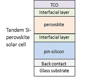
Our joint research aims at realizing a tandem solar cell combining a small band gap silicon absorber with a higher band gap material called organometal halide perovskites. The Information Device Science Laboratory (NAIST) and the LPICM (Ecole Polytechnique, CNRS) have complementary expertise in different areas related to photovoltaic energy, both in terms of materials processing and in characterization tools.
In a longer term, one goal of these tandem cells is to combine them with an earth-abundant electrolyzer for production of hydrogen, as a way of storing solar energy in a clean fuel.
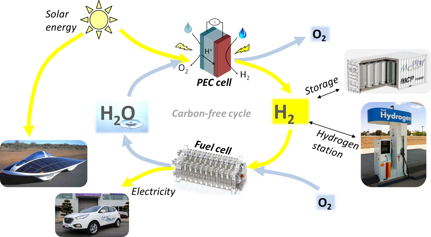
Carbon-free energy cycle for the storage of solar energy in hydrogen from solar-powered water splitting. Hydrogen is an energy carrier which has a very high mass energy density, but it must be used under high pressures (700 bar) because hydrogen at atmospheric pressure has a low volume energy density compared to liquid fuels. Hydrogen can be stored and transported before being distributed in fuel stations to hydrogen cars, which uses hydrogen in a fuel cell to recover energy as electricity with only water as a byproduct.
Information Device Science Laboratory
The Information Device Science Laboratory is conducting research on the information function devices that can support the next-generation information society. Many daily necessities around us such as TV sets, personal computers, and mobile phones, are composed of silicon-based semiconductor devices. Its research features the introduction of various new materials on silicon substrates, its own unique designs, and production of semiconductor devices that make the best use of their features. Producing semiconductor devices with innovative functions on the basis of skilled manufacturing is the main goal of this laboratory with applications in next-generation high-tech information terminals, LSIs with new functions based on biological supramolecules, printed/flexible displays using wide band gap materials, printing technology for energy harvesting devices (solar cell, thermoelectric devices), and emerging devices (Graphene transistors, power devices based on GaN). The know-how of the laboratory goes from material formation using varied processing methods to characterization (structure, optical and electrical properties, and simulation), for a wide range of applications.
Laboratory of Physics of Interfaces and Thin Films
LPICM has long time experiences with the deposition of thin film materials using plasma enhanced chemical vapor deposition techniques, development of devices and optical characterization tools. The plasma reactors developed at LPICM have been used to develop materials including silicon passivation layers and absorbers for solar cells, nanowires for photovoltaic and battery applications, carbon nanotubes and graphene for sensors, etc. The know-how of the laboratory contains also experiences with fabrication of organic, hybrid materials and devices, including perovskites and OLED devices by wet and evaporated process. Laboratory is also known for its long term devotion to the development of new characterization tools for microelectronics, biomedical applications and material science, including commercialized Mueller matrix polarimeter, NanoRaman setup and confocal colposcope for cancer diagnosis. The strong background of the laboratory in the material and device research and fabrication is supported by numerous characterization techniques of material and device properties, such as EQE, ellipsometry, Mueller matrix polarimetry, solar simulator, AFM (including CAFM and KAFM), Raman spectroscopy (on micro and nanoscale), photoluminescence, SEM, TEM, etc.