
Optical holograms are widely used in our daily life as certificates on credit cards for example. 3D structure information is recorded in the optical hologram based on the nature of light as a wave. Similarly, 3D atomic arrangement can be recorded using electron waves. The photoelectron wave emitted from an atom by x-ray excitation is partially scattered by the surrounding atoms. As a result, an interference pattern between direct and scattered waves, photoelectron hologram, is formed. Photoelectron holography (PEH) is the powerful method for studying surface and subsurface atomic structures in 3D owing to the short probing depth of photoelectrons. The 3D images of atomic arrangements around the photoelectron emitter atom are directly obtained from the element-specific holograms.
Graphite intercalation compounds (GIC) are old and new superconducting materials. The highest transition temperature (Tc) value for the GIC superconductors at ambient pressure is currently 11.5 K for CaC6. Recently, a new series of bimetal-intercalated graphite superconductors, CaxK1-xCy, was successfully fabricated by Prof. Y. Kubozono group at Okayama University. As K and Ca atoms intercalated, a graphite flake turned to a golden superconducting compound. The Tc of KC8 was only 136 mK, but the introduction of a very small amount of Ca drastically increased this value. The Tc of CaxK1-xCy continuously increased to 11.5 K (x=1; CaC6) nonlinearly as x increased.
Direct visualization of three-dimensional (3D) atomic arrangements around intercalant atoms is essential to clarify the superconducting mechanism. X-ray diffraction is a standard method to determine bulk crystal structure, but not suitable for the local structure analysis of non-periodic alloy compounds. Moreover, the cleaved surface of GICs are readily degraded by moisture and oxygen in the atmosphere. The local structure around the intercalant atoms of bimetal GIC superconductors remained unclear.
We have measured photoelectron spectra and holograms using a two-dimensional display-type analyzer installed at the circularly polarized soft X-ray beamline BL25SU. A superconducting (Ca,K)C8 sample (Tc=9.9 K) was recently prepared by Kubozono group. We made a vacuum sample transfer system between Okayama and SPring-8 in order to prevent the degradation of the samples. The photoelectron spectra of the cleaved surface of (Ca,K)C8 showed only C 1s and K 2p peaks, and the Ca 2p peak intensity was less than a few hundredths of that of the K 2p peak. The observation of the K dominant structure at the cleaved surface implies that Ca atoms are dispersed in the bulk and likely form high Tc domains.
Full hemisphere C 1s and K 2p photoelectron holograms are shown in the figure. From these holograms, we directly reconstructed atomic images from the few-layer region of cleaved surface. These observations revealed that the cleavage preferentially occurs at the K atom intercalated layers containing no Ca atoms, which is likely the most fragile part of the crystal sample. The most important result from the present study is that the cleaved surface does not always represent the averaged bulk structure. The structure and composition of the surface and the bulk can be substantially different, especially in a layered system. Special attention must be paid when using surface-sensitive methods, such as photoelectron spectroscopy and scanning probe microscopy.
Recently, superconductivity of In and Pb monoatomic layers and GIC and FeSe ultra-thin films on surfaces has been discovered and has attracted substantial fundamental interest. The crystal size of newly developed functional materials is often very small and the density of impurity atoms playing important roles are low. As mentioned above, PEH is one of the most effective methods for studying surface and subsurface atomic structures in 3D. This technique for directly visualizing atomic arrangement by the element selective PEH is expected to be a powerful tool for new superconducting material development.
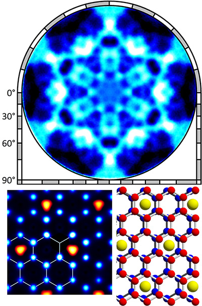
(top) C 1s photoelectron hologram from (Ca,K)Cy.
(bottom left) Atomic arrangement image of C (blue) and K (orange) layers.
(bottom right) Structure model of the cleaved surface region of (Ca,K)Cy.
Title: "Photoelectron Holographic Atomic Arrangement Imaging of Cleaved Bimetal-intercalated Graphite Superconductor Surface"
Publication: Fumihiko Matsui, Ritsuko Eguchi, Saki Nishiyama, Masanari Izumi, Eri Uesugi, Hidenori Goto, Tomohiro Matsushita, Kenji Sugita, Hiroshi Daimon, Yuji Hamamoto, Ikutaro Hamada, Yoshitada Morikawa, Yoshihiro Kubozono; Scientific Reports, 6, 36258, published online 4 November 2016
DOI: http://dx.doi.org/10.1038/srep36258![]()
naistar: http://hdl.handle.net/10061/11096![]() (NAIST Academic Repository:naistar)
(NAIST Academic Repository:naistar)