
The international collaboration team consisting of Prof. Munetaka Taguchi and Prof. Hiroshi Daimon of the Nara Institute of Science and Technology, Dr. Masaki Oura of the RIKEN SPring-8 Center, Dr. G. Panaccione of the Istituto Officina dei Materiali-CNR, Laboratorio and Prof. G. van der Laan of Diamond Light Source (United Kingdom), succeeded in quantitatively evaluating the depth distribution of the surface inactive layer, which prevents us from making a new spintronic devices. The international team combined the world's highest performance X-ray photoelectron spectroscopy experiment in two synchrotron radiation facilities, Diamond (UK) and SPring-8 (Japan), and theoretical analysis for this study. It can be expected that research on development for the spintronic devices will be greatly promoted, as the quantitative and nondestructive measurement of the layer structure of the inactive layer became possible. The results of this research will be published in the UK science e-journal "Nature Communications" (July 17 [Press release deadline: July 17 (Monday, July 17th, 2007 at 6:00 pm)).
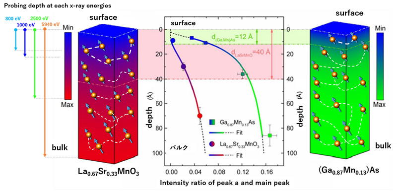
Depth distribution of surface inactive layer for La0.67Sr0.33MnO3 and (Ga0.87Mn0.13)As
【Paper title and author(s)】
- Title: Quantifying the critical thickness of electron hybridization in spintronics materials.
- Publication: T. Pincelli, V. Lollobrigida, F. Borgatti, A. Regoutz, B. Gobaut, C. Schlueter, T. -L. Lee, D. J. Payne, M. Oura, K. Tamasaku, A. Y. Petrov, P. Graziosi, F. Miletto Granozio, M. Cavallini, G. Vinai, R. Ciprian, C. H. Back, G. Rossi, M. Taguchi, H. Daimon, G. van der Laan and G. Panaccione; Nature Communications, Volume 8, 16051, 17 July 2017.
- DOI: http://dx.doi.org/10.1038/ncomms16051